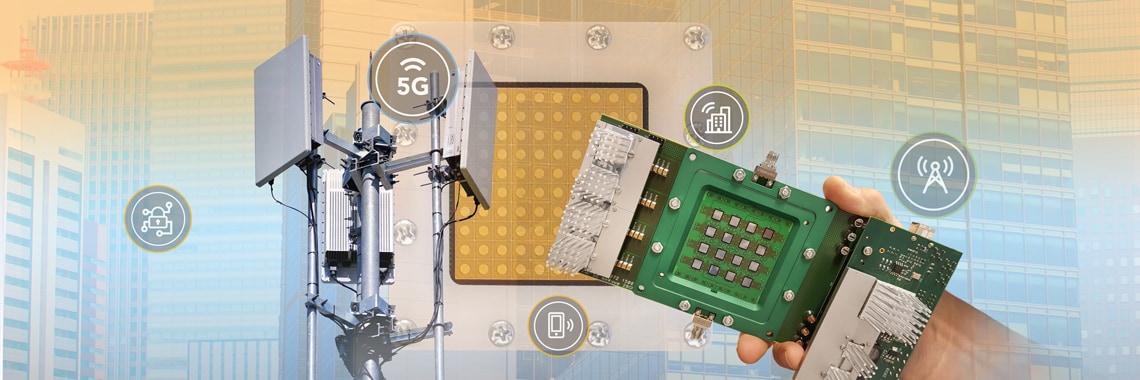
Telecommunication Base Station PCBs: Innovations for 5G
As the global rollout of 5G technology accelerates—projected to reach over 60% of the world's population by 2030—the evolution of base station printed circuit boards (PCBs) is imperative. These innovations are crucial for addressing the demanding requirements of faster, more efficient telecommunications infrastructure. In this article, we will delve into the emerging trends and innovations in PCB technology that are paving the way for the future of telecommunication base stations.
Compact Designs: The Shift to High-Density Interconnect (HDI) Technology
As urban environments grow denser, telecommunication base stations must become more compact. High-density interconnect (HDI) technology is playing a pivotal role in this shift. HDI allows for a greater number of components to be packed into smaller spaces using microvias and finer trace widths, often as narrow as 50 micrometers. This is particularly essential for base stations that need to support multiple frequency bands and advanced antenna systems within a limited footprint.
The trend towards miniaturization not only enhances functionality but also aligns with the demands of modern, space-constrained urban landscapes. As engineers adopt HDI technology, they can ensure that base stations remain effective without sacrificing quality or performance.
Effective Thermal Management: Innovations to Prevent Overheating
With base stations operating continuously at high power levels—often exceeding 100 watts per module—effective thermal management becomes crucial. Overheating can lead to equipment failure and compromised reliability, making advanced thermal solutions a priority in PCB design.
Innovations such as metal-core PCBs and embedded heat sinks are gaining traction. These designs use materials with high thermal conductivity, like aluminum or copper, to dissipate heat efficiently. By integrating these thermal management solutions into PCB designs, manufacturers can significantly enhance the longevity and reliability of telecommunication equipment.
Flexible PCBs for Antenna Modules
Another significant trend in the design of telecommunication PCBs is the increasing use of flexible PCBs, particularly in antenna modules. Flexible PCBs can wrap around components, saving space while maintaining signal integrity. Constructed from polyimide materials, these boards can withstand bending without cracking, ensuring reliable performance even in dynamic environments.
This flexibility is especially valuable in the deployment of small cell base stations, which are commonly placed in urban corners, on streetlights, and even integrated into buildings. The ability to maintain integrity while fitting into unconventional shapes allows for more versatile installation options, thus enhancing network coverage in densely populated areas.
Sustainability in PCB Manufacturing
As environmental concerns grow, sustainability has become a focal point in PCB manufacturing. Manufacturers are exploring halogen-free materials and recyclable substrates to mitigate the environmental impact while maintaining performance standards. The shift toward eco-friendly materials aligns with stricter regulations on hazardous substances and responds to consumer demand for greener technologies.
By adopting sustainable practices, PCB manufacturers can not only reduce their environmental footprint but also appeal to a market increasingly focused on corporate responsibility and ecological stewardship.
Challenges and Opportunities Ahead
While these technological advancements are promising, challenges persist in designing efficient PCBs for telecommunication base stations. Signal integrity remains a significant concern at high frequencies, with issues such as crosstalk and impedance mismatches affecting performance. To counteract these problems, designers are implementing controlled impedance techniques and utilizing advanced simulation software to identify potential issues before manufacturing.
Additionally, the cost of advanced materials and technologies can hinder large-scale deployment. To navigate this barrier, manufacturers are optimizing designs by using hybrid materials—combining high-performance substrates only where necessary while utilizing more economical options elsewhere. This approach ensures that the performance does not come at an exorbitant cost.
The Future of Telecommunication Networks
As the telecommunications landscape continues to evolve rapidly, the integration of cutting-edge technologies in PCB design will be crucial for creating reliable and efficient networks. By investing in innovations such as HDI technology, effective thermal management, flexible designs, and sustainable practices, engineers and manufacturers are setting the groundwork for the next generation of telecommunication infrastructure.
By embracing these technologies today, the industry can build a foundation for faster, more reliable, and more sustainable telecommunication networks tomorrow. As we move toward a more connected world, the role of telecommunication PCBs will only grow in importance, underpinning the entire 5G ecosystem and beyond.
References
For more detailed insights into current trends and innovations in PCB technology, visit ALLPCB.